


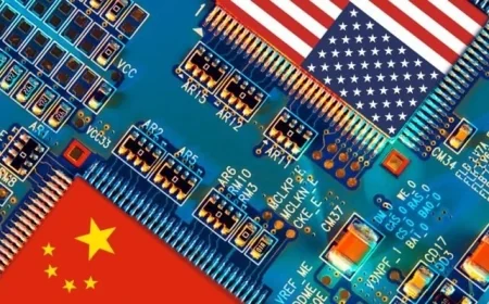


US Startup Substrate Unveils Chipmaking Tool to Challenge ASML and TSMC Dominance
SAN FRANCISCO, Oct 28 — American startup Substrate announced on Tuesday that it has developed a breakthrough chipmaking tool capable of competing with the world’s most advanced lithography machines—a domain long dominated by Dutch tech giant ASML. The innovation marks the first step in Substrate’s bold plan to build a U.S.-based contract chip manufacturing business, directly rivaling Taiwan Semiconductor Manufacturing Company (TSMC) in producing next-generation AI chips.

A Disruptive Bid to Reclaim Chipmaking Leadership
Founded and led by James Proud, Substrate aims to dramatically cut chip production costs by manufacturing critical fabrication tools domestically and more affordably than existing global suppliers. “At some point, everyone just gave up on the chip problem and accepted the TSMC-ASML duopoly,” said Paul Kwan, Managing Director at General Catalyst, one of Substrate’s early backers.
The company’s rise aligns with President Donald Trump’s push to bring semiconductor manufacturing back to U.S. soil. The administration recently took a stake in Intel, as part of a broader national security and economic strategy to reduce reliance on Asia for advanced chips.
Substrate has raised $100 million in funding at a valuation exceeding $1 billion, with backing from In-Q-Tel—the CIA’s venture capital arm—as well as General Catalyst, Allen & Co, Long Journey Ventures, and Valor Equity Partners.
Challenging the ASML Monopoly
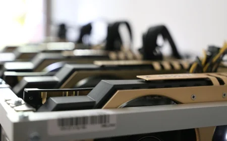
Lithography—the process of using light to etch microscopic circuit patterns onto silicon wafers—is among the most complex feats in modern engineering. ASML remains the only company capable of mass-producing extreme ultraviolet (EUV) lithography tools, each costing over $400 million and indispensable for fabricating the world’s most advanced chips.
Substrate claims to have developed a novel X-ray-based lithography system capable of printing semiconductor features at resolutions comparable to ASML’s EUV tools—but at a fraction of the cost. The company says it has successfully demonstrated its system at U.S. National Laboratories and its San Francisco facilities, sharing high-resolution imaging results to verify the tool’s precision.
Reuters noted, however, that it could not independently verify Substrate’s technical claims.
National and Economic Stakes
“This is an opportunity for the U.S. to recapture this market with a homegrown company,” said Stephen Streiffer, Director of Oak Ridge National Laboratory and an expert in X-ray technologies. “It’s a nationally important effort—and they know what they’re doing.”
If Substrate succeeds in slashing lithography and fabrication costs, analysts say the effect could mirror SpaceX’s transformation of the space industry. “It could have second-order effects across the entire semiconductor supply chain,” said Jeff Koch, an analyst at SemiAnalysis.
Still, the road ahead is steep. Building a full-scale chip fabrication ecosystem that can rival TSMC requires billions in capital and deep technical expertise. Modern fabs can cost upwards of $15 billion each, and even giants like Intel and Samsung have struggled to perfect next-generation processes.
Balancing Independence and Collaboration
While Substrate has not received direct government funding, CEO Proud confirmed that U.S. officials have been closely following the company’s progress. “It’s really important that what we’re doing is commercially viable on its own,” he said, adding that Commerce Secretary Howard Lutnick and other administration officials have been engaged “from the very start.”
Substrate’s long-term ambition is to establish a domestic alternative to Asia’s manufacturing giants—reducing dependency, enhancing national security, and potentially redefining global chip economics.